






| 모델 P/N | 시리즈 | 실험실/CLBS 수 | 속도 등급 | 논리 요소/셀 수 | 총 램 비트 | I/O 수 | 전압 - 공급 | 마운팅 유형 | 작동 온도 | 패키지 / 케이스 | 공급업체 디바이스 패키지 |
|---|---|---|---|---|---|---|---|---|---|---|---|
| XC7Z045-L2FBG676E | Zynq-7000 SoC | 27,33 | 0,00 | ~350,000 LE | 19200000 | 250 | 1.0 V | SMD/SMT | 0 °C ~ +100 °C | FCBGA-676 | FCBGA-676 |
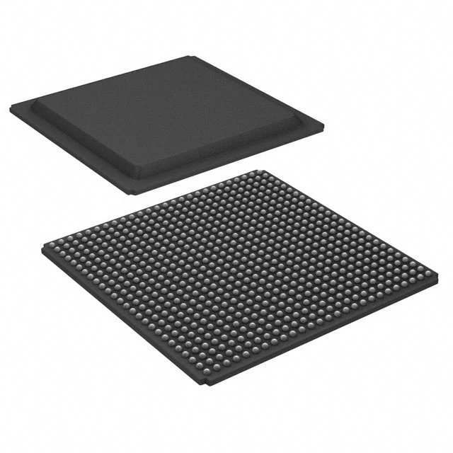
사양
Part Number Explanation
This is Xilinx Zynq-7000 high-end heterogeneous all-programmable SoC built on 28nm process, integrating dual-core Cortex-A9 processor and Kintex-7 class large-scale FPGA logic, tailored for low-power, wide-temperature rugged industrial, vehicular and airborne embedded systems.
- XC7Z045: Top-tier high-capacity device of Zynq-7000 family, equipped with Kintex-series FPGA resources
- L2: Low-power optimized speed grade 2; supports reduced core voltage operation to lower static and dynamic power consumption while retaining reliable timing performance
- FBG676: 676-ball flip-chip FCBGA compact packaging
- E: Extended industrial temperature grade, junction temperature range: -40°C ~ +125°C
Complete On-Chip Hardware Architecture
1. Processing System (PS: ARM Subsystem)
- Dual-core ARM Cortex-A9 MPCore, maximum operating frequency up to 1000MHz
- Each core: 32KB instruction cache + 32KB data cache; 1MB shared L2 cache
- Integrated NEON SIMD floating-point accelerator for signal processing, audio and image computing acceleration
- Rich built-in peripherals: Dual Gigabit Ethernet, USB 2.0 OTG, SD/MMC, CAN bus, UART, SPI, I2C, general GPIO
- Secure boot supported to prevent program tampering and ensure system safety
2. Programmable Logic (PL: Kintex-7 FPGA Fabric)
- Total Logic Cells: 354,560
- DSP48E1 dedicated arithmetic blocks: 1920 units, ideal for large-scale FFT, digital filtering, wireless baseband preprocessing, multi-channel image algorithm acceleration and matrix computation
- Total Block RAM capacity: 19.2 Mb
- Multiple MMCM & PLL clock management tiles for multi-clock generation and clock jitter suppression
- No embedded high-speed serial transceivers inside the chip
3. I/O Interfaces & On-Chip Analog Monitoring
- Available user configurable I/O pins: 360
- Adjustable I/O bank voltage ranging from 1.2V to 3.3V, compatible with LVCMOS, LVDS, HSTL and mainstream differential signaling standards
- On-chip dual-channel 12-bit XADC: real-time monitoring of die temperature, internal power supply voltages and external analog input signals
전원 공급 장치 사양
Standard core voltage: 1.0V
Low-power mode enables voltage reduction to cut overall power consumption under light workloads
Separate independent power domains for PS processor part and PL FPGA logic part
Typical total power consumption: 11W ~ 32W; passive heat sinks are applicable for compact rugged embedded devices
포장 및 SMT 조립 요건
- Package: 676-pin flip-chip FCBGA ball grid array
- Moisture Sensitivity Level: MSL3; all reflow soldering work must be completed within 168 hours after vacuum packaging is opened
- Lead-free design, fully RoHS compliant
- Delivered in anti-static trays for automated PCB mass production
Environmental & Reliability Features
Capable of stable long-term operation under drastic temperature changes and intense electromagnetic interference industrial environments.
Supports bitstream encryption protection and SEU single-event upset error detection, built for harsh outdoor industrial equipment, automotive electronic control units, portable field measuring instruments and lightweight airborne electronic systems requiring wide temperature adaptability and high stability.
일반적인 애플리케이션 시나리오
- Outdoor rugged industrial controllers, field edge gateway and remote monitoring terminals
- Vehicular multi-channel data recording, automotive visual perception and in-vehicle video processing units
- Handheld high-precision signal analyzers, portable vibration and environmental monitoring acquisition instruments
- Miniature airborne short-range radar signal preprocessing, onboard lightweight data forwarding modules
- Rugged field portable machine vision inspection equipment
- Wide-temperature industrial-grade SOM core boards and rugged embedded secondary development platforms


