| 모델 P/N | 시리즈 | 실험실/CLBS 수 | 속도 등급 | 논리 요소/셀 수 | 총 램 비트 | I/O 수 | 전압 - 공급 | 마운팅 유형 | 작동 온도 | 패키지 / 케이스 | 공급업체 디바이스 패키지 |
|---|---|---|---|---|---|---|---|---|---|---|---|
| XC4VLX25-10FFG668C | Virtex-4 SX | 2.688,00 | 0,00 | 24192 논리 요소 | 1,327,104비트 | 448 | 1.14V ~ 1.26V | 표면 실장 | 상업용(0°C ~ +85°C) | 668-BBGA, FCBGA | 668-FCBGA(27×27) |
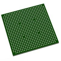
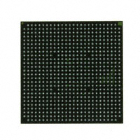
XC4VLX25-10FFG668C: Virtex-4 LX Logic-Optimized FPGA
그리고 XC4VLX25-10FFG668C is a fundamental component of the Xilinx Virtex-4 LX platform, designed specifically for logic-intensive applications. Built on a 90nm process using triple-oxide technology, the LX series balances high logic density with managed power consumption.
그리고 -10 speed grade 그리고 Commercial temperature rating make this part an ideal fit for high-performance networking, medical imaging backplanes, and industrial automation controllers that require stable, high-speed logic without the overhead of the SX (DSP-heavy) or FX (embedded PowerPC) variants.
Essential Technical Specifications
로직 셀: 24,192
CLB Array: 48 x 72
Total Block RAM: 1,296 Kb
DSP48 Slices: 48
최대 사용자 I/O: 448
패키지: FFG668 (Flip-Chip BGA, Lead-Free/RoHS)
속도 등급: -10
작동 온도 0°C ~ +85°C(상업용)
Design & Integration Insights
When designing with or sourcing the LX25 in the FFG668 package, several architectural nuances should be considered:
SelectIO Technology: This device supports multiple I/O standards (LVDS, HSTL, SSTL). Designers should pay close attention to the banking rules—specifically, ensuring that the $V_{CCO}$ of a given bank is compatible with all I/O standards assigned to that bank to avoid signal integrity issues.
Clock Management: The Virtex-4 LX features highly flexible Digital Clock Managers (DCMs). For the -10 speed grade, ensure your timing constraints in ISE account for the specific jitter and setup/hold requirements documented in the DS302 datasheet.
Thermal Design: The Flip-Chip (FFG) package offers lower thermal resistance than traditional wire-bond BGAs. However, even at a -10 grade, high logic utilization at high frequencies can lead to significant localized heating. We recommend verifying junction temperature ($T_j$) through thermal simulation if your design exceeds 70% logic utilization.
Hardware Engineer FAQ
Is the XC4VLX25-10FFG668C pin-compatible with larger Virtex-4 LX devices?
Yes, the FFG668 package allows for footprint compatibility with the XC4VLX40 and XC4VLX60 in some configurations, permitting a migration path if your logic requirements grow. Always cross-reference the pinout tables to ensure bank-compatible power pins.
How should I handle the lead-free (FFG) soldering profile?
Since this is a Lead-Free (RoHS) FFG668 package, you must follow a SAC305-compatible reflow profile. Avoid using leaded solder pastes if you require full RoHS compliance for your final assembly.
What is the status of the “Silicon Stepping” for this part?
We supply the latest production steppings. For engineers performing FFF (Form, Fit, Function) replacements on older Rev A or B boards, please verify if your existing bitstream requires a “Stepping-specific” update via ISE.
LXB 세미콘에 문의 for availability, pricing, and technical support.


