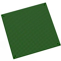
| 모델 P/N | 시리즈 | 실험실/CLBS 수 | 속도 등급 | 논리 요소/셀 수 | 총 램 비트 | I/O 수 | 전압 - 공급 | 마운팅 유형 | 작동 온도 | 패키지 / 케이스 | 공급업체 디바이스 패키지 |
|---|---|---|---|---|---|---|---|---|---|---|---|
| XC4VLX200-10FFG1513I | Virtex-4 LX | 22.272,00 | -10,00 | 200448 | 6193152 | 960 | 1.14V ~ 1.26V | 표면 실장 | -40 °C ~ +100 °C (Industrial) | 1513-BBGA (FCBGA) | 1513-FCBGA |
XC4VLX200-10FFG1513I: The Apex of High-Density Logic & Industrial Reliability
그리고 XC4VLX200-10FFG1513I represents the maximum logic capacity available in the Xilinx Virtex®-4 LX series. Engineered for massive system integration, this FPGA is designed for architects who need to consolidate complex multi-processor systems, extensive DSP arrays, and high-speed switching fabrics into a single silicon footprint.
As an Industrial-grade (-I) device with a Lead-Free (FFG1513) package, it provides the ultimate combination of environmental resilience and massive I/O throughput.
Engineering Core Capabilities
Maximum Logic Scale: Boasting a staggering 200,448 Logic Cells, the LX200 allows for the deployment of multiple heavy-duty IP cores (such as PCIe, Ethernet MACs, and soft-core processors) without reaching routing saturation.
Superior Memory Density: Features over 6Mbit (6,048 Kb) of Block RAM. This massive on-chip storage is critical for deep packet buffering, high-resolution video frame buffers, and large-scale FFT implementations.
High-Pin-Count Connectivity: Housed in the 1513-pin Flip-Chip BGA, this device breaks out 960 User I/Os. This allows for the simultaneous management of multiple high-width memory interfaces (DDR2/QDR) and wide parallel system buses.
Industrial Thermal Range: Specifically binned for -40°C to +100°C junction temperature operation. This ensures timing stability and logic integrity in mission-critical environments where active cooling may be limited or ambient temperatures fluctuate.
Advanced XtremeDSP™ Resources: Includes 96 DSP48 slices, providing high-performance hardware acceleration for arithmetic-intensive applications like radar signal processing and medical imaging.
Technical Specification Matrix
| 기능 | 사양 |
| 논리 셀 | 200,448 |
| CLB Array | 22,512 |
| Total Block RAM | 6,048 Kb |
| DSP48 Slices | 96 |
| User I/Os | 960 |
| 속도 등급 | -10 |
| 온도 등급 | 산업용(-40°C ~ +100°C) |
| 패키지 | FFG1513 (Lead-Free Flip-Chip BGA) |
Why Specify the LX200-10FFG1513I?
1. Unmatched Logic Consolidation
If you are moving away from multi-FPGA boards to a single-chip solution, the LX200 is the industry standard for Virtex-4 designs. The massive logic-to-I/O ratio eliminates the latency penalties and board complexity associated with inter-FPGA communication.
2. Robust Signal Integrity
그리고 FFG1513 package is engineered with a high density of power and ground pins to mitigate Simultaneous Switching Noise (SSN). Even when toggling hundreds of I/Os at high speeds, the device maintains clean signal eyes and robust noise margins.
3. Long-Term Reliability & Compliance
The “FFG” lead-free designation ensures your product meets modern RoHS compliance while the “Industrial” rating provides the necessary overhead for long-lifecycle deployment in telecommunications backbones and ruggedized control systems.
High-Value Applications
Communications: 10G/40G networking line cards and base station processing.
Defense & Aerospace: Radar beamforming, UAV signal processing, and secure communication.
Scientific Computing: ASIC emulation, hardware-in-the-loop (HIL) testing, and genomic sequencing acceleration.
Medical: Real-time 3D reconstruction for CT and MRI systems.


