






| Mfr 부품 | 데이터시트 | 시리즈 | 제조업체 | 패키지 | 토폴로지 | 제품 상태 | 마운팅 유형 | 스위칭 주파수 | 기능 | 입력 전압 | 출력 전압 | 출력 개수 | 작동 온도 | 출력 유형 | 출력 전류 |
|---|---|---|---|---|---|---|---|---|---|---|---|---|---|---|---|
| LTC7149EUFD |  |
LTC7149 | 아날로그 디바이스 | 28-QFN | Buck | 활성 | 표면 실장 | 400kHz - 3MHz | DC-DC 레귤레이터 | 3.4V - 36V | 조정 가능 | 1 | -40°C ~ +125°C | 조정 가능 | 20 A |
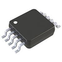
사양
부품 번호 정의
LTC7149 refers to high-voltage synchronous inverting step-down DC-DC regulator dedicated for negative voltage generation. E denotes commercial extended temperature grade. UFD stands for 28-lead QFN surface mount package with exposed thermal pad, sized 4mm × 5mm. This part is available in tube or tape-and-reel formats for prototype verification and mass automated SMT assembly.
주요 전기적 성능 매개변수
This fully integrated synchronous monolithic buck converter is optimized for positive input to negative output voltage conversion. It accepts an ultra-wide input voltage range from 3.4V up to 60V, and generates adjustable negative output voltage ranging from 0V down to -28V, with maximum continuous inductor current rated at 4A. The output voltage is precisely set via one single external resistor, delivering ±0.8% tight output accuracy across all working conditions.
Two N-channel power MOSFETs are embedded inside the chip, featuring typical on-resistance of 110mΩ (top switch) and 50mΩ (bottom switch), supporting peak conversion efficiency up to 92%. Two operational modes are optional: Burst Mode for elevated efficiency under light load conditions, and forced continuous mode for minimized output ripple and low electromagnetic noise. External clock synchronization is supported to eliminate frequency interference among multiple power rails on the same PCB.
Switching frequency can be programmed between 300kHz and 3MHz by an external resistor, enabling designers to adopt small-size inductors and capacitors for compact power solutions. Key current consumption parameters include 440μA no-load quiescent current and 15μA shutdown current. A programmable soft-start circuit restricts inrush current during power-on startup.
Built-in comprehensive protection functions cover thermal shutdown, output short-circuit protection, overcurrent limiting, and power-good voltage monitoring. All logic control pins are ground-referenced, requiring no extra level shifting circuits for simple MCU/FPGA control. Internal or external loop compensation is selectable to adapt to diverse output filter configurations.
포장 및 조립 사양
Housed in miniature 28-pin QFN package with central exposed thermal pad, overall dimensions 4mm × 5mm × 0.75mm. The exposed pad delivers superior thermal conductivity to dissipate heat efficiently under full-load continuous operation, suppressing internal junction temperature rise drastically. Moisture Sensitivity Level is MSL3; all reflow soldering processes must be completed within 168 hours once the original vacuum packaging is unsealed. Both tube and tape reel delivery options are offered to satisfy manual debugging and high-volume production demands.
환경 및 규정 준수 기준
The operating junction temperature range spans -40°C to +125°C, enabling reliable continuous operation in industrial instrumentation, automotive electronic control systems, telecommunication terminals, laboratory test equipment and portable measurement devices exposed to dramatic temperature variations. Manufactured with lead-free materials, the component complies with global RoHS environmental directives. Full integration of power switches and control circuitry reduces peripheral passive component count, simplifies PCB layout and shortens power supply development cycle.
일반적인 애플리케이션 분야
Dual-polarity analog power supply generation for industrial precision instruments
Automotive electronic system negative bias voltage power modules
OLED, LCD display panels and audio amplifier negative voltage power rails
Portable high-precision test & measurement equipment multi-rail power conversion circuits
Wide-input remote telecommunication terminal negative output power supplies


