






| Mfr 부품 | 데이터시트 | 시리즈 | 제조업체 | 패키지 | 토폴로지 | 제품 상태 | 마운팅 유형 | 스위칭 주파수 | 기능 | 입력 전압 | 출력 전압 | 출력 개수 | 작동 온도 | 출력 유형 | 출력 전류 |
|---|---|---|---|---|---|---|---|---|---|---|---|---|---|---|---|
| LT3045EDD#TRPBF |  |
LT3045 | 아날로그 디바이스(선형) | DFN-10 | LDO 레귤레이터 | 활성 | SMD | N/A | 초저잡음 LDO | +1.8V~+20V | 조정 가능 | 1 | -40°C ~ +125°C | 규제 | 500mA |
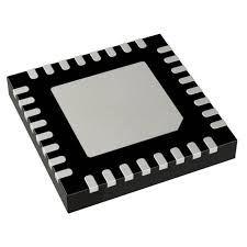
사양
부품 번호 정의
LT3045 is an ultra-low noise, high PSRR low-dropout linear regulator developed by Analog Devices. E denotes industrial extended temperature grade specification. DD stands for 10-lead 3mm×3mm thermally enhanced DFN surface mount package. #TRPBF means 7-inch tape-and-reel lead-free packaging designed for high-volume automated SMT mass production.
주요 전기적 성능 매개변수
This premium LDO adopts a unique architecture combining precision current reference and high-performance voltage buffer, specifically optimized for powering noise-sensitive analog, RF and high-precision conversion circuits. Multiple devices can be easily paralleled to further reduce output noise, boost total output current and distribute thermal load evenly across PCB traces.
The input voltage ranges from 1.8 V up to 20 V, delivering a maximum continuous output current of 500 mA with a typical dropout voltage of only 260 mV at full load. Output voltage is adjustable from 0 V to 15 V via a single external resistor; thanks to unity-gain internal configuration, output noise, PSRR, bandwidth and load regulation performance remain nearly consistent regardless of the set output voltage.
Key noise and rejection indicators: total output noise is merely 0.8 μV RMS within 10 Hz to 100 kHz bandwidth, spot noise reaches 2 nV/√Hz at 10 kHz, and power supply rejection ratio hits 76 dB at 1 MHz, effectively suppressing high-frequency switching ripple from upstream DC-DC converters.
Quiescent supply current is 2.2 mA under normal operation, and drops below 1 μA in shutdown mode for idle power saving. It integrates programmable current limit, fast startup sequence and programmable power-good indicator to monitor regulated output status. Stable operation is guaranteed with only a 10 μF minimum ceramic output capacitor.
Comprehensive built-in protection mechanisms cover reverse battery protection, reverse current protection, foldback current limiting and hysteretic thermal shutdown to prevent chip damage caused by abnormal wiring and overload conditions.
포장 및 조립 사양
Encapsulated in compact 10-pin DFN plastic package with exposed thermal pad, dimensioned 3 mm × 3 mm. The central exposed pad offers excellent heat dissipation capability to lower junction temperature during continuous full-load operation. Moisture Sensitivity Level is MSL3; all reflow soldering procedures must be finished within 168 hours after the original vacuum packaging is opened. Continuous tape reel feeding is configured to fully match the automatic placement machine workflow for mass manufacturing.
환경 및 규정 준수 기준
Industrial operating temperature range spans -40 °C to +125 °C, supporting reliable long-term operation in laboratory precision instruments, medical diagnostic equipment, wireless communication RF modules and high-end audio devices under severe temperature fluctuations. Manufactured with lead-free materials, the component complies with global RoHS environmental directives. The streamlined peripheral circuit layout reduces passive component count and simplifies ultra-clean power rail design for precision analog systems.
일반적인 애플리케이션 분야
Power supply for high-resolution ADC, DAC and analog front-end signal conditioning circuits
RF system power rails including VCO, PLL, LNA and mixer modules for communication equipment
High-fidelity audio DAC, headphone amplifier ultra-low noise power supplies
Medical ultrasonic diagnostic instruments and MRI peripheral analog power circuits
Portable precision test measurement equipment and laboratory calibration power sources


