






| Mfr 부품 | 데이터시트 | 시리즈 | 제조업체 | 패키지 | 토폴로지 | 제품 상태 | 마운팅 유형 | 스위칭 주파수 | 기능 | 입력 전압 | 출력 전압 | 출력 개수 | 작동 온도 | 출력 유형 | 출력 전류 |
|---|---|---|---|---|---|---|---|---|---|---|---|---|---|---|---|
| ADG509AKRZ |  |
ADG | 아날로그 디바이스 | SOIC-16 | 아날로그 멀티플렉서 | 활성 | SMD | N/A | 듀얼 4:1 MUX | ±5V ~ ±15V 또는 +10.8V-+16.5V | N/A | 2 | -40°C ~ +85°C | 아날로그 | N/A |
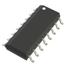
사양
부품 번호 정의
ADG509A is a dual 4-channel differential CMOS analog multiplexer. K represents extended industrial temperature grade. RZ stands for 16-lead narrow-body SOIC surface mount package, delivered in tube packaging for prototype circuit verification, debugging and small-batch equipment assembly.
주요 전기적 성능 매개변수
Fabricated with enhanced LC²MOS monolithic CMOS technology, this device integrates two independent single-pole four-throw switching arrays, which is designed to switch four pairs of differential analog input signals to a single differential output port. Channel selection is implemented via two address pins together with a global enable pin, and all digital control inputs are fully compatible with TTL and 5V CMOS logic standards.
The device supports flexible power supply configurations: single supply ranging from 10.8 V to 16.5 V, or dual bipolar supplies of ±10.8 V to ±16.5 V, with an absolute maximum voltage rating up to 44 V. Analog input signals can swing fully from negative supply rail to positive supply rail without signal clipping.
The maximum on-resistance of each internal switch is 450 Ω, while the maximum on-resistance mismatch between different channels is limited to 22.5 Ω. Turn-on and turn-off switching times both equal 300 ns, enabling fast channel switching operations. Typical off-state leakage current is 20 pA with a maximum value of 1 nA, which effectively preserves measurement accuracy for low-amplitude analog signals. Charge injection is controlled at only 4 pC, and low parasitic capacitance minimizes waveform distortion during signal routing.
Total maximum power dissipation is 28 mW for low quiescent power consumption. On-chip frequency compensation ensures stable operation across all closed-loop gain configurations without external compensation components, making it suitable for low-frequency and mid-frequency analog signal switching applications. Excellent channel isolation restrains crosstalk between two differential signal paths.
포장 및 조립 사양
Housed in a compact 16-lead narrow SOIC plastic surface mount package with a body width of 3.9 mm, occupying minimal PCB layout space for miniaturized analog signal acquisition modules. Moisture Sensitivity Level is MSL1; there is no time restriction on reflow soldering after opening the vacuum sealed package. Tube packaging facilitates manual breadboard testing, circuit performance validation and small-volume pre-production assembly.
환경 및 규정 준수 기준
The operating temperature range covers -40 °C to +85 °C, supporting continuous reliable operation inside industrial control cabinets, laboratory bench measuring instruments, outdoor environmental monitoring terminals and other environments with wide temperature variation and electromagnetic interference. Manufactured using lead-free production processes, the component complies with global RoHS environmental directives. The highly integrated single-chip architecture eliminates numerous discrete peripheral components, simplifies the hardware design of differential analog front-end circuits and accelerates product development cycles.
일반적인 애플리케이션 분야
Multi-channel differential sensor signal multiplexing circuits for industrial temperature, pressure and process variable monitoring
Front-end analog switching modules for high-precision data acquisition systems
Range switching circuitry for digital multimeters and laboratory bench measurement devices
Multiplexed low-level signal sampling paths for portable field inspection instruments
Differential audio signal routing and analog conditioning circuits for compact medical diagnostic equipment


