






| Mfr 부품 | 데이터시트 | 시리즈 | 제조업체 | 패키지 | 토폴로지 | 제품 상태 | 마운팅 유형 | 스위칭 주파수 | 기능 | 입력 전압 | 출력 전압 | 출력 개수 | 작동 온도 | 출력 유형 | 출력 전류 |
|---|---|---|---|---|---|---|---|---|---|---|---|---|---|---|---|
| ADG2128BCPZ |  |
ADG2128 | 아날로그 디바이스 | 16-TSSOP | 아날로그 스위치 | 활성 | 표면 실장 | — | 아날로그 스위치 | 3V - 13.2V | — | 1 | -40°C ~ +85°C | 아날로그 | — |
사양
부품 번호 정의
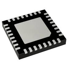
ADG2128 is an 8 × 12 bidirectional analog crosspoint switch array controlled via I2C bus. B denotes standard industrial temperature grade specification. CPZ stands for 32-lead 5mm × 5mm exposed pad LFCSP surface mount package. This component is supplied in tube packaging for prototype verification, circuit evaluation and small-batch production assembly.
주요 전기적 성능 매개변수
This monolithic CMOS analog matrix switch contains total 96 independent switching channels arranged in 12 rows and 8 columns. The entire array is fully bidirectional, so both row terminals and column terminals can be flexibly defined as signal input or output ports according to system routing requirements.
All internal switches are individually addressed and configured through an I2C-compatible serial interface, supporting three transmission rates including standard 100kHz, full-speed 400kHz and high-speed 3.4MHz. Built-in dual buffer logic enables synchronous state update of multiple switches via dedicated commands, and a hardware reset pin can turn off all switching channels instantly. All switches remain open-circuit after power-up to avoid unexpected signal conduction.
The device can operate under dual ±5V bipolar power rails or single 12V power supply with complete electrical parameter characterization. Maximum on-resistance is limited to 35 ohms, bringing minimal signal attenuation during transmission. The -3dB bandwidth reaches up to 300MHz, which guarantees high-fidelity routing for high-speed analog signals such as video waveforms. Typical quiescent supply current is less than 20μA for low idle power consumption. Excellent channel isolation and low parasitic capacitance effectively suppress crosstalk between different signal paths.
포장 및 조립 사양
Encapsulated in compact 32-pin thermally enhanced LFCSP plastic package with overall dimension 5mm × 5mm and central exposed thermal pad. The exposed pad improves heat dissipation efficiency and offers stable grounding connection to optimize high-frequency signal performance. Moisture Sensitivity Level is MSL3; all reflow soldering procedures must be completed within 168 hours once the original vacuum packaging is unsealed. Tube delivery mode is adopted to facilitate manual breadboard debugging, performance testing and small-volume equipment trial manufacturing.
환경 및 규정 준수 기준
The operating temperature range covers -40°C to +85°C, enabling stable continuous operation in automotive infotainment systems, medical ultrasonic imaging devices, communication equipment and laboratory test instruments under variable temperature and electromagnetic interference environments. The component has passed automotive reliability certification and is manufactured with lead-free processes to comply with global RoHS environmental directives. Highly integrated single-chip architecture eliminates massive discrete analog switching components, simplifies multi-channel analog routing PCB layout and shortens product hardware development cycle.
일반적인 애플리케이션 분야
Automotive infotainment audio and video signal switching modules
Medical ultrasound beamforming multi-channel signal routing circuits
Telecommunication PBX system analog voice path matrix switches
KVM equipment and CCTV surveillance video signal distribution units
Bench-top test and measurement instrumentation multi-channel analog multiplexing systems
Home audio-video receiver signal selection and distribution circuits


