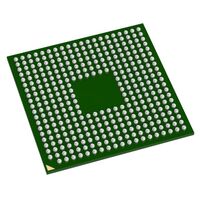
| МОДЕЛЬ П/Н | СЕРИИ | КОЛИЧЕСТВО ЛАБОРАТОРИЙ/КЛБ | УРОВЕНЬ СКОРОСТИ | КОЛИЧЕСТВО ЛОГИЧЕСКИХ ЭЛЕМЕНТОВ / ЯЧЕЕК | ВСЕГО БИТОВ ОЗУ | КОЛИЧЕСТВО ВХОДОВ/ВЫХОДОВ | НАПРЯЖЕНИЕ - ПИТАНИЕ | ТИП КРЕПЛЕНИЯ | РАБОЧАЯ ТЕМПЕРАТУРА | УПАКОВКА / КЕЙС | УПАКОВКА УСТРОЙСТВА ПОСТАВЩИКА |
|---|---|---|---|---|---|---|---|---|---|---|---|
| XC4VLX25-11SFG363C | Virtex-4 SX | 2.688,00 | -11,00 | 24192 Логические элементы | 1 327 104 бит | 240 | 1,14 V ~ 1,26 V | Монтаж на поверхность | Коммерческий (0°C ~ +85°C) | 363-FBGA, FCBGA | 363-FCBGA (17×17) |
XC4VLX25-11SFG363C: High-Performance Virtex-4 LX in a Compact 17mm Footprint
Сайт XC4VLX25-11SFG363C is a logic-optimized FPGA within the Xilinx Virtex-4 LX family, specifically binned for the -11 speed grade. This device is the ideal solution for high-speed logic applications—such as LVDS data concentration, PCIe bridging, or high-frequency state machines—where board real estate is at a premium.
By utilizing the SFG363 package, this FPGA delivers over 24k logic cells in a small-form-factor BGA. The -11 speed grade provides roughly a 10-15% performance improvement over the base -10 version, allowing for easier timing closure on complex, high-frequency designs.
Core Technical Specifications
Логические ячейки: 24,192
Max Clock Management Tiles (CMTs): 8
Блок оперативной памяти: 1,296 Kb
DSP48 Slices: 48
Max User I/O: 240
Упаковка: SFG363 (17mm x 17mm, 0.8mm ball pitch, Lead-Free/RoHS)
Класс скорости: -11 (High Performance)
Temperature Grade: Коммерческий (от 0°C до +85°C)
Engineering Implementation & Design Considerations
1. Timing Margin and the -11 Speed Grade
The -11 speed grade is critical for designs operating near the upper frequency limits of the 90nm Virtex-4 architecture. If your design is failing to meet setup time ($T_{su}$) in a -10 speed grade, the XC4VLX25-11 provides the necessary slack. However, always re-run your Static Timing Analysis (STA) in ISE to ensure that hold times ($T_h$) remain compliant, as the faster silicon reduces propagation delays across the fabric.
2. SFG363 Routing Challenges
The 0.8mm ball pitch of the SFG363 package is significantly tighter than the 1.0mm pitch used in the 668-pin variants.
PCB Stack-up: Ensure your PCB vendor can support the required trace widths and clearances for BGA breakout.
Via-in-Pad: Depending on your density, via-in-pad technology may be required to access the inner I/O rings while maintaining signal integrity for high-speed differential pairs.
3. Legacy Toolchain Compatibility
The XC4VLX25-11SFG363C is a mature component and is not supported by Xilinx Vivado. Maintenance and new bitstream generation require Xilinx ISE Design Suite 14.7. When migrating designs, verify that your .ucf constraints reflect the SF363 pinout, as it is not pin-compatible with the larger FFG668 footprint.
Comparison: Virtex-4 LX25 – Speed & Package Options
| Характеристика | XC4VLX25-11SFG363C | XC4VLX25-10SFG363C |
| Степень скорости | -11 (Faster) | -10 (Standard) |
| Logic Performance | Higher Timing Margin | Standard Logic |
| Пакет | 17mm SFG363 | 17mm SFG363 |
| I/O Count | 240 | 240 |
Hardware Engineer’s FAQ
Can I use the XC4VLX25-11SFG363C as a drop-in replacement for the -10 speed grade?
Yes. Xilinx FPGAs are backward compatible regarding speed grades. A -11 part will meet or exceed all timing requirements of a -10 part. Note that while timing improves, you should monitor localized thermal density if the part is running at significantly higher toggle rates.
What is the “G” in the SFG363 package name?
The “G” designates a Lead-Free (RoHS compliant) package. This is the standard for modern assembly, though it requires a slightly different reflow profile compared to the older leaded (SF363) versions.
Why is the I/O count only 240 compared to other LX25 parts?
The LX25 die has more I/O capability, but the SF363 package is physically too small to bond out all available signals. This is a deliberate trade-off for size. If your design requires more than 240 I/Os, you must migrate to the FFG668 package.
Looking for verifiable stock or an official quote?
We specialize in sourcing mature-market Xilinx silicon with full traceability. We understand that for legacy infrastructure, getting the exact speed grade and package is non-negotiable for system stability.
Would you like me to pull the specific IBIS models or the Pin-to-Pin delay tables for this -11 speed grade part?
Связаться с LXB Semicon for availability, pricing, and technical support.


