






XCZU27DR-2FFVG1517I
Produsen: AMD (Xilinx)
Saluran ADC RFSoC: 16
Saluran DAC RFSoC: 16
Paket: FFVG1517
Suhu Pengoperasian: Industri (-40°C hingga +100°C)
Spesifikasi
Definisi Nomor Bagian
This is a Zynq UltraScale+ RFSoC heterogeneous multiprocessor SoC developed by AMD Xilinx, built on the 16nm FinFET manufacturing process. It integrates ARM processing subsystem, programmable FPGA logic fabric and on-chip RF analog converters, positioned for medium and small-scale wireless communication, portable radar and software defined radio applications.
- XCZU27DR: Mid-entry tier RFSoC device with integrated high-speed RF ADC/DAC modules
- -2: Speed Grade 2, high-performance timing grade with sufficient timing margin for baseband algorithm development
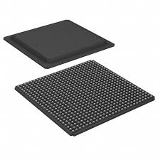
- FFVG1517: 1517-ball flip-chip FCBGA package
- I: Industrial temperature grade, operating junction temperature range: -40°C ~ +100°C
Complete On-Chip Hardware Architecture
1. Processing System (PS: ARM Processor Domain)
- Quad-core ARM Cortex-A53 application processors, tasked with running Linux OS, upper-layer communication protocol stacks and application management
- Dual-core lockstep ARM Cortex-R5F real-time cores for high-security low-latency control tasks and system fault monitoring
- Integrated Mali-400 MP2 GPU for lightweight graphical interface rendering
- Dedicated hardware video codec engine supporting multi-channel video encoding and decoding
- Abundant standard peripherals: dual Gigabit Ethernet, USB 3.0, SD interface, CAN bus, UART, SPI, I2C
- Built-in hardware security unit for secure boot, 256-bit AES encryption and intellectual property anti-tampering protection
2. Programmable Logic Fabric (PL: FPGA Domain)
- Total Logic Cells: 444,000
- DSP48E2 arithmetic blocks: 1728 units, applied to FFT operations, digital filtering, channel equalization, matrix computation and wireless baseband signal processing
- Total Block RAM + UltraRAM storage: 32.76 Mbit
- Multiple MMCM and PLL clock management tiles, supporting clock multiplication, division, phase shifting and jitter reduction to satisfy multi-clock domain system design demands
- Configurable I/O banks compatible with LVCMOS, LVDS and various differential signaling standards
3. Integrated RF Analog Subsystem (Core RFSoC Feature)
On-chip integrated high-speed radio frequency sampling converters, removing the need for external discrete analog chips and simplifying RF hardware layout:
- 8-channel 14-bit ADC, maximum per-channel sampling rate: 5 GSPS
- 8-channel 14-bit DAC, maximum per-channel update rate: 10 GSPS
- Embedded digital up converters (DUC), digital down converters (DDC) and automatic gain control modules for on-chip RF signal frequency conversion and gain adjustment
4. Transceiver Serial Berkecepatan Tinggi
16 GTY differential high-speed transceivers, maximum single-lane line rate up to 32.75 Gbps. Compatible with PCIe Gen4, 100G Ethernet, JESD204B/C protocols for high-speed inter-device data transmission.
Spesifikasi Catu Daya
Independent power domains are assigned to the processing system, programmable logic, RF analog circuits and high-speed transceivers. Typical core logic voltage is 0.85 V; dynamic voltage and frequency scaling is supported to adjust power consumption based on runtime load.
Typical overall power consumption ranges from 16 W to 38 W, requiring passive heat sinks or forced air cooling solutions.
Packaging & SMT Assembly Specifications
- Package type: 1517-pin flip-chip FCBGA ball grid array
- Moisture Sensitivity Level: MSL3. All reflow soldering work must be completed within 168 hours after vacuum packaging is opened
- Lead-free construction, fully compliant with global RoHS environmental regulations
- Packaged in anti-static trays for automated large-scale industrial PCB assembly
Environmental and Reliability Characteristics
Capable of stable long-term operation under drastic temperature variations and intense electromagnetic interference environments.
Equipped with 256-bit AES bitstream encryption, anti-tampering design, SEU radiation error correction and dual R5F lockstep redundant operation, meeting high reliability requirements for military, aerospace and outdoor wireless devices.
Skenario Aplikasi Umum
- 5G/6G indoor small cell base stations and distributed radio access equipment
- Portable software-defined radio (SDR) and wireless signal test transceiver platforms
- Miniature phased array radar, ranging radar front-end and echo signal processing terminals
- Portable electronic warfare signal reconnaissance, monitoring and interception devices
- Aerospace airborne short-range communication and remote sensing signal acquisition equipment
- Mid-range spectrum analyzers, portable vector signal generators and communication test instruments


