






| الطراز P/N | السلسلة | عدد المعامل/المختبرات | درجة السرعة | عدد العناصر/الخلايا المنطقية | إجمالي بتات ذاكرة الوصول العشوائي (RAM) | عدد الإدخال/الإخراج | الجهد - الإمداد | نوع التركيب | درجة حرارة التشغيل | العبوة / العلبة | حزمة جهاز المورد |
|---|---|---|---|---|---|---|---|---|---|---|---|
| XC7K420T-L2FLG901E | كينتكس-7 | 32.575,00 | -2,00 | 416,960 | 30781440 | 380 | 0.97 - 1.03 فولت (النوع 1.0 فولت) | التركيب على السطح | 0 درجة مئوية - 100 درجة مئوية | 901-FCBGA | 901-FCBGA |
XC7K420T-L2FLG901E
الشركة المصنعة: زيلينكس
الخلايا المنطقية: 419,840
شرائح المنطق: 65,600
ذاكرة الوصول العشوائي المدمجة (eRAM): 30,240 كيلو بايت (840 × 36 كيلو بايت من ذاكرة الوصول العشوائي المجمعة)
الحد الأقصى لإدخال/إخراج المستخدم: 400
الحزمة: FFG901 (Flip-Chip BGA)
درجة السرعة: -2 لتر
درجة حرارة التشغيل: ممتد (من 0 درجة مئوية إلى +100 درجة مئوية)
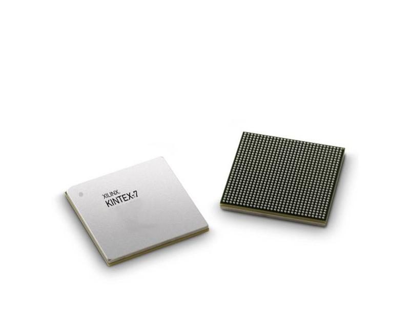
المواصفات
تعريف رقم القطعة
This extended commercial temperature FPGA belongs to Xilinx Kintex-7 product family, built on mature 28nm HKMG semiconductor process with unified 7-series optimized architecture. It balances logic scale, DSP computing performance, high-speed serial bandwidth and overall cost, designed for indoor communication devices, laboratory signal test equipment, video processing systems and wired transmission hardware working under stable indoor ambient temperature.
- XC7K420T: Large-capacity mainstream model of Kintex-7 series, positioned for medium-to-large digital system development, delivering balanced performance and power consumption for industrial and communication scenarios
- L2: Low-power grade 2 timing specification. Optimized for static and dynamic power consumption, power efficiency and thermal stability are prioritized over maximum operating clock frequency, suitable for long-running indoor devices with limited heat dissipation conditions
- FFG901: 901-ball flip-chip FCBGA package. The package structure provides excellent heat dissipation performance and signal integrity, sufficient pins support full layout of all integrated GTX transceivers, general I/O ports and multi-channel DDR3 memory interfaces
- E: Extended commercial temperature range, continuous junction temperature working scope: 0°C ~ +100°C
معلمات موارد الأجهزة المدمجة في الرقاقة
1. موارد المنطق القابل للبرمجة
- Total Logic Cells: 423,360
- Available CLB Slices: 65,850
- Flip-Flop Count: 1,317,000
- LUT Count: 658,500
- Distributed RAM: 6.01 Mb
2. Arithmetic & Embedded Memory Resources
- DSP48E1 arithmetic units: 1,680 pieces, applied to fixed-point and floating-point operations, FFT spectrum analysis, communication baseband processing, radar signal calculation and encryption algorithm acceleration
- Block RAM total capacity: 30.85 Mb, used for video frame buffering, deep FIFO cache, waveform data storage and algorithm parameter table storage
3. نظام إدارة الوقت
- 10 MMCM clock modules
- 10 حلقات قفل الطور (PLL)
Multiple independent clock domains can be configured freely. The system supports accurate clock phase adjustment, transmission delay compensation and low jitter suppression, meeting strict timing synchronization demands of large-scale digital signal processing and communication systems
4. أجهزة الإرسال والاستقبال التسلسلية عالية السرعة
- 32 GTX high-speed differential transceivers
Maximum single-lane rate reaches 12.5 Gbps, compatible with PCIe Gen2, 10 Gigabit Ethernet, Aurora, JESD204B and mainstream industrial high-speed serial protocols. Built-in hard protocol controllers shorten the development cycle of high-bandwidth data transmission interfaces
5. واجهات الإدخال/الإخراج ووحدة المراقبة المدمجة في الرقاقة
- User configurable I/O pins: 400
Multiple I/O power banks ranging from 1.2V to 3.3V are supported, fully compatible with LVCMOS, LVDS, HSTL, SSTL and all common single-ended and differential signal standards
Built-in XADC monitoring module continuously detects chip junction temperature, internal core voltage and external analog signals in real time
خصائص مصدر الطاقة
Core supply voltage for L2 low-power version is optimized for power saving. Logic arrays, block RAM, DSP units and serial transceivers are divided into independent power domains, supporting partial module power shutdown to flexibly reduce overall power consumption
Typical total power consumption range: 15W ~ 40W. Continuous full-load operation at upper temperature limit requires forced air cooling configuration
مواصفات التغليف وتجميع المكونات السطحية (SMT)
- Package Type: 901-pin Flip-Chip BGA
- مستوى الحساسية للرطوبة: MSL4. يجب إتمام جميع عمليات اللحام بإعادة التدفق في غضون 72 ساعة بعد فتح العبوة المفرغة من الهواء
- Lead-free packaging design, fully compliant with RoHS environmental standards
- Devices are stored and transported in anti-static trays to avoid electrostatic damage during mass PCB production
Environmental Adaptability and Reliability
This chip is designed for constant-temperature indoor environments. It can run stably for a long time under mild temperature fluctuations, slight mechanical vibration and conventional electromagnetic interference. It supports bitstream AES encryption, dynamic partial reconfiguration and SEU error detection and correction. Without radiation-hardened design, it cannot work normally under outdoor low temperature and harsh rugged environments.
سيناريوهات التطبيق النموذجية
- 10G/40G optical communication line cards, enterprise room switching and routing main control boards
- Laboratory spectrum analyzers, arbitrary waveform generators and multi-channel high-speed data acquisition equipment
- Industrial 4K video encoding and decoding equipment, high-precision machine vision image processing platforms
- Medium-scale digital chip prototype verification and communication algorithm development platforms for research institutions
- Indoor industrial high-speed data gateways and desktop lightweight encryption acceleration hardware


