






| الطراز P/N | السلسلة | عدد المعامل/المختبرات | درجة السرعة | عدد العناصر/الخلايا المنطقية | إجمالي بتات ذاكرة الوصول العشوائي (RAM) | عدد الإدخال/الإخراج | الجهد - الإمداد | نوع التركيب | درجة حرارة التشغيل | العبوة / العلبة | حزمة جهاز المورد |
|---|---|---|---|---|---|---|---|---|---|---|---|
| XC7K420T-L2FLG1156E | كينتكس-7 | 32.575,00 | -2,00 | 416,960 | 30781440 | 400 | 0.97 ~ 1.03 | التركيب على السطح | 0 درجة مئوية ~ 100 درجة مئوية (ه) | 1156-FCBGA | 1156-FCBGA (35×35) |
XC7K420T-L2FLG1156E
الشركة المصنعة: زيلينكس
الخلايا المنطقية: 419,840
شرائح المنطق: 65,600
ذاكرة الوصول العشوائي المدمجة (eRAM): 30,240 كيلو بايت (840 × 36 كيلو بايت من ذاكرة الوصول العشوائي المجمعة)
الحد الأقصى لإدخال/إخراج المستخدم: 500
الحزمة: FFG1156 (Flip-Chip BGA)
درجة السرعة: -2 لتر
درجة حرارة التشغيل: ممتد (من 0 درجة مئوية إلى +100 درجة مئوية)
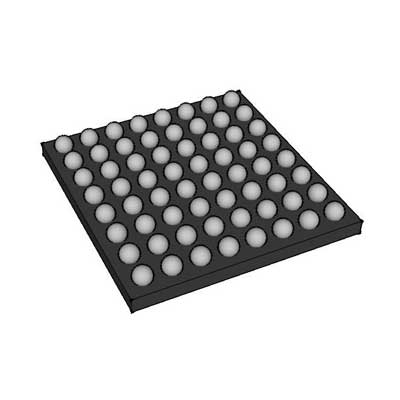
المواصفات
تفصيل أرقام القطع
This is a low-power extended industrial temperature high-density FPGA based on Xilinx Kintex-7 architecture, built on mature 28nm semiconductor manufacturing process. It integrates abundant logic resources, massive DSP arithmetic units and multiple high-speed serial ports, tailored for rugged airborne, vehicular, outdoor communication and portable precision test equipment that demand low power consumption, wide temperature stability and powerful parallel computing capability.
- XC7K420T: High-density flagship model of Kintex-7 series, the suffix T stands for low-power optimized silicon variant
- L2: Low-power optimized Speed Grade 2. Core operating voltage is reduced to cut static and dynamic power consumption greatly; timing performance is stable across full temperature range while balancing clock frequency and power budget
- FFG1156: 1156-ball flip-chip FCBGA large-size package. Sufficient pins reserve space for massive parallel I/O, multi-group high-speed transceivers and extended peripheral circuits
- E: Extended industrial temperature specification, operating junction temperature range: -40°C ~ +100°C
On-Chip Hardware Resource Allocation
1. الموارد العامة للمنطق القابل للبرمجة
- Total Logic Cells: 424,000
- Available Configurable Slices: 66,250
- Total Flip-Flops: 530,000
- Total LUT Lookup Tables: 265,000
2. موارد الحساب والذاكرة المدمجة
- DSP48E1 dedicated arithmetic slices: 1,620 units, applicable to large-scale FFT operations, digital filtering, radar echo signal processing, multi-channel video algorithm acceleration and high-order matrix computation
- Total Block RAM Storage: 29,880 Kb, used for large image frame buffering, deep FIFO data queues, waveform caching and algorithm parameter storage tables
- Distributed RAM Capacity: 7,360 Kb
3. النظام الفرعي لإدارة الساعة
- 10 وحدات إدارة التوقيت MMCM
- 10 حلقات قفل الطور (PLL)
Supports multi-clock domain generation, phase fine adjustment, clock delay compensation and high-frequency jitter suppression, meeting strict timing synchronization requirements of complex large-scale digital systems
4. أجهزة الإرسال والاستقبال التسلسلية عالية السرعة
- 16-channel GTX high-speed differential transceivers
Maximum achievable line rate up to 10.3125 Gbps, compatible with PCIe Gen2, 10G Ethernet, CPRI, JESD204B, Aurora mainstream serial communication standards
5. I/O Interfaces & Built-In Monitoring Module
- User configurable general I/O pins: 560
I/O bank supply voltage adjustable from 1.2V to 3.3V, fully supports LVCMOS, LVDS, HSTL, SSTL and all mainstream differential signal standards
Dual-channel 12-bit XADC analog acquisition module is integrated on chip, which continuously monitors die internal junction temperature, all internal power rail voltages and external analog input signals in real time
مواصفات مصدر الطاقة
Nominal core logic voltage under low-power mode: Lowered standard 1.0V core voltage
Logic fabric, embedded RAM, DSP array and high-speed transceivers adopt independent isolated power domains respectively
Typical overall power consumption range: 11W ~ 34W; compact active cooling solution can satisfy long-term full-load stable operation under high-temperature working conditions
Packaging & SMT Assembly Standards
- Package Type: 1156-pin flip-chip FCBGA ball grid array
- Moisture Sensitivity Level: MSL4; all reflow soldering procedures must be completed within 72 hours after vacuum packaging is unsealed
- Lead-free packaging design, fully compliant with RoHS environmental protection directives
- Delivered and stored in anti-static trays to prevent electrostatic damage during automated PCB mass production
Environmental Adaptability & Operational Reliability
The chip can run continuously and stably under extreme temperature swings, mechanical vibration, shock and moderate electromagnetic interference harsh environments. It supports 256-bit AES bitstream encryption protection and SEU single-event upset error detection & correction, with enhanced thermal robustness for long-term field deployment.
سيناريوهات التطبيق النموذجية
- Portable high-end spectrum analyzers, multi-channel high-speed oscilloscopes and signal recording instruments
- Software-defined radio baseband processing platforms, outdoor small cell communication equipment
- Multi-channel industrial machine vision inspection control systems, high-speed image real-time processing units
- Vehicular multi-sensor fusion computing main controllers, automotive intelligent edge computing terminals
- Lightweight airborne radar signal preprocessing, flight data acquisition and forwarding modules
- Wide-temperature low-power high-performance industrial SOM core boards and complex embedded algorithm verification platforms


